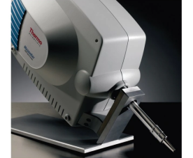
Electron Microscopes (EM) use a beam of accelerated electrons in order to generate an image, the electrons used having a shorter wavelength than that of visible or UV light used in optical light microscopes. The very nature of the electron allows for higher magnification and better resolution. Electron microscopes fall into two basic categories – transmission electron microscopes (TEM) and scanning electron microscopes (SEM). Due to their powerful resolution and the possibility of magnification, they have found application in material characterization, semiconductor production and life science.
– Various electron microscopy techniques used in material characterization have been proven in different fields of material research such as: fundamental research on metals, quality control and failure analysis, battery, polymer and geological research, oil and gas, nanoparticles, forensics, catalysis research, fibers and filters, automotive materials testing, as well as 2D materials research.
– EM methods in life sciences including large volume analysis, cryo-electron microscopy (cryo-EM), cryo-tomography and single particle analysis have found their application in structural biology, infectious disease, drug discovery, plant biology, pathology and cancer research.
– Consistent improvements in performance and energy efficiency of both semiconductor and microelectronic devices are enabled with EM, which include semiconductoer pathfinding and development, yield ramp and metrology, failure analysis, physical and chemical characterization, ESD qualification as well as power semiconductor device analysis.
Electron Microscopy Applications
SKU: 11231
Available in countries :
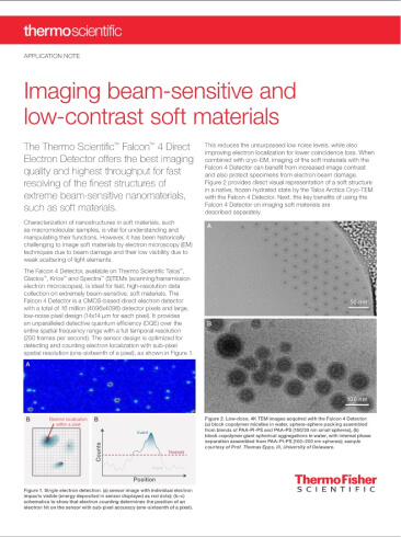
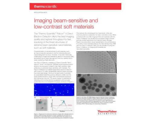
TEM: Imaging beam-sensitive and low-contrast soft materials
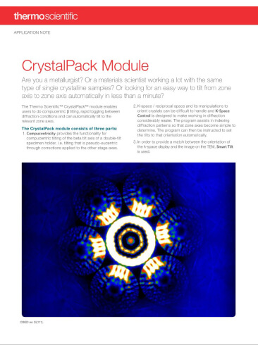
TEM: CrystalPack Module
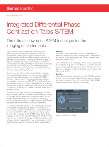
TEM: Integrated Differential Phase Contrast on Talos S/TEM
ETEM: Environmental Transmission Electron Microscopy
ETEM: Use of an Environmental Transmission Electron Microscope for Dynamic in situ Studies of Nano-Structured Materials at the Atomic Scale
ETEM: Atomic scale structure-function relationship of heterogeneous catalysts: investigation of gassolid interactions by ETEM
TEM: Fringe-Free Imaging (FFI)
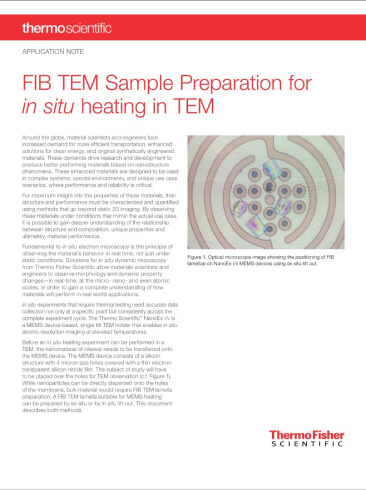
DBeam: FIB TEM Sample Preparation for in situ heating in TEM
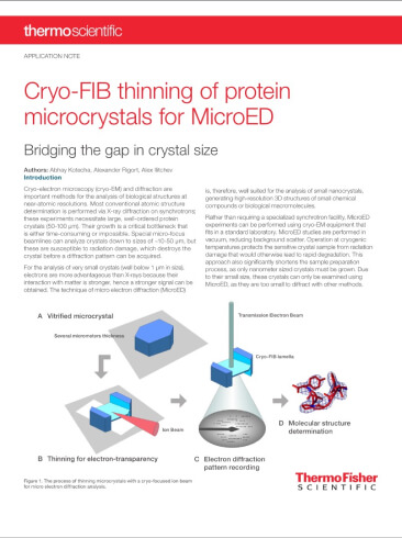
DBeam: Cryo-FIB thinning of protein microcrystals for MicroED
DBeam: Spin Mill method for large-area planar milling
DBeam: Large area automated sample preparation for batteries
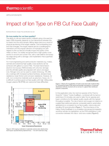
DBeam: Impact of Ion Type on FIB Cut Face Quality
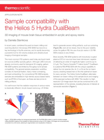
DBeam: Sample compatibility with the Helios 5 Hydra DualBeam
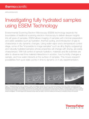
SEM: Investigating fully hydrated samples using ESEM Technology
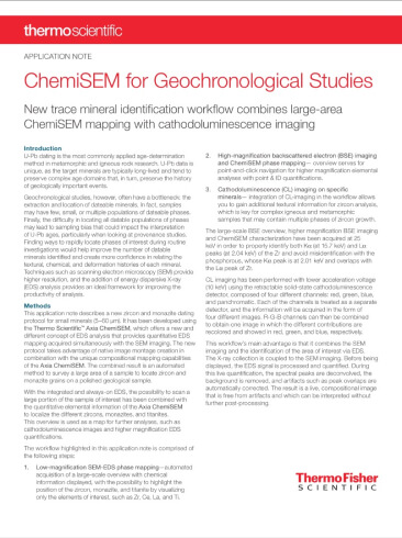
SEM: ChemiSEM for Geochronological Studies
SEM: Microstructural and chemical evaluation of a thermally cycled thermal barrier coating system
SEM: Characterization of complex refractories for steel production using the Axia ChemiSEM
SEM: Failure analysis of corroded steel surface
SEM: Malachite characterization with Axia ChemiSEM
SEM: Characterization of tire fillers with Axia ChemiSEM
SEM: Assessment of contaminants within battery materials via Axia ChemiSEM
SEM: Bend failure mechanism of high-strength steel
SEM: Characterization of glass fiber-reinforced polymers with ChemiSEM Technology
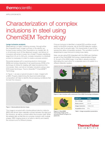
SEM: Characterization of complex inclusions in steel using ChemiSEM Technology
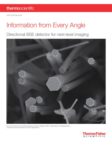
SEM: Information from Every Angle
SEM: Extreme High Resolution Electron Microscopy
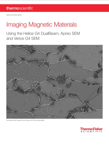
SEM: Imaging Magnetic Materials
