


ESCALAB Xi+ X-ray Photoelectron Spectrometer (XPS) Microprobe

Nexsa G2 Surface Analysis System

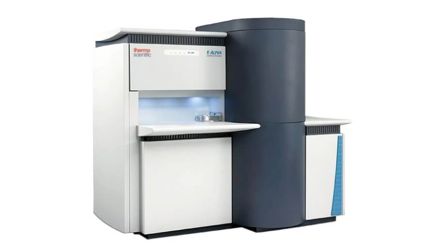
K-Alpha X-ray Photoelectron Spectrometer System

FAQ - X-ray Photoelectron Spectroscopy (XPS)
XPS is based on the photoelectric effect, in which X-rays cause electrons to be emitted from the surface of a material. By measuring their kinetic energy, electron binding energies can be determined, enabling elemental identification and analysis of chemical states.
XPS is a highly surface-sensitive technique that typically provides information from the top few nanometers of a material, approximately 1–10 nm, depending on the sample and measurement conditions. This makes it particularly suitable for analyzing thin surface layers, contamination, oxidation, and surface chemical modifications.
In addition to elemental composition, XPS provides information about oxidation states and different chemical environments of elements. Shifts in binding energy can be used to distinguish certain chemical states, such as metallic and oxidized forms of an element.
Conventional XPS can detect most chemical elements except hydrogen and helium. Sensitivity depends on the element, its chemical environment, concentration, and instrument characteristics. XPS is particularly useful for determining surface elemental composition and chemical states.
XPS enables identification of elemental chemical states in surface oxide layers on metals. This allows oxidation, passivation, and corrosion processes to be investigated. The technique is useful for studying protective coatings, surface treatments, and metal degradation mechanisms.
Depth profiling enables investigation of chemical composition changes through material surface layers. Controlled ion sputtering is commonly used to remove material gradually, with XPS measurements performed between sputtering steps. Potential changes in sample chemistry caused by sputtering must be considered.
XPS determines chemical composition, oxidation states, and surface contamination in thin films and coatings. With appropriate methods, composition changes with depth can also be investigated. This analysis is important for developing functional coatings, electronic components, and protective layers.
XPS analysis is performed under high or ultra-high vacuum to minimize collisions between emitted electrons and gas molecules and to limit surface contamination. Stable vacuum conditions enable precise electron energy measurements and reliable surface composition analysis.
A chemical shift is a change in electron binding energy caused by differences in an atom’s chemical environment. Analyzing these shifts makes it possible to distinguish certain oxidation states and chemical bonding environments. This is one of the main advantages of XPS over techniques that determine only elemental composition.
In battery research, XPS is used to characterize electrode surfaces, protective layers, and changes in chemical states during operation. In the semiconductor industry, it enables analysis of thin films, oxide layers, and surface contamination, supporting the development and reliability of electronic components.