
Scanning Electron Microscopy (SEM)
Since the introduction of electron microscopes in the 1930s, scanning electron microscopy (SEM) has developed into a critical tool within numerous different research fields, spanning areas from materials science, to forensics, to industr...
Read more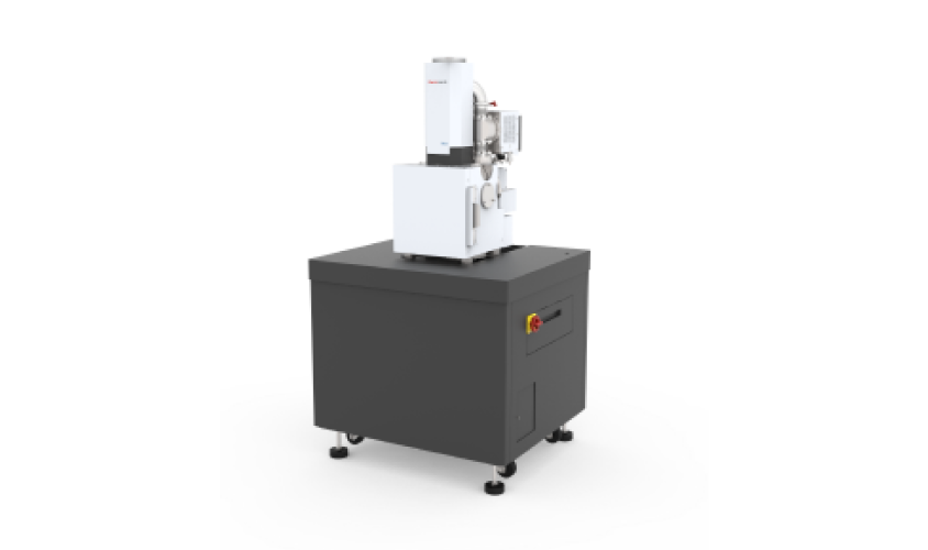
Desktop Scanning Electron Microscopy (Desktop SEM)
Since the introduction of electron microscopes in the 1930s, scanning electron microscopy (SEM) has developed into a critical tool within numerous different research fields, spanning areas from materials science, to forensics, to industr...
Read more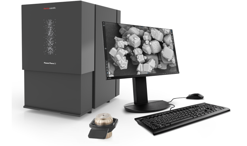
Transmission electron microscopy (TEM)
Transmission electron microscopy (TEM) is a high-resolution imaging technique in which an image is produced when a beam of electrons passes through a thin sample. The electron beam is impacted by the thickness/density of a sample, its co...
Read more
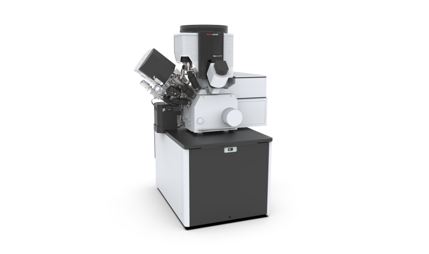
DualBeam Instruments
DualBeam - focused ion beam scanning electron microscopy (FIB-SEM) instruments generate structural and compositional information at the nanoscale, by combining the precise sample modification of FIB with the high-resolution imaging of SE...
Read more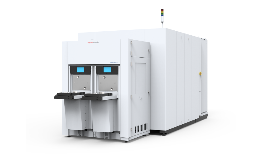
Electrical Failure Analysis (EFA) Systems
Shrinking technologies, new materials, and more complex structures are making defects increasingly common - especially when the circuit design is particularly sensitive to process variation. These non-visual defects reveal themselves as ...
Read more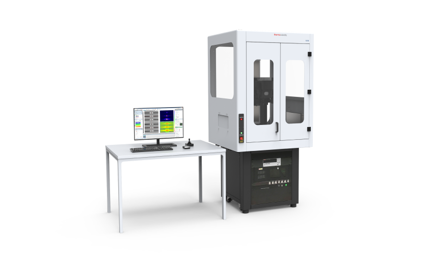
Circuit Edit Systems
Circuit edit technology enables fast prototyping of small design corrections at multiple points of the IC manufacturing process: after first silicon debug, for performance enhancements during yield ramp, to create a small number of funct...
Read more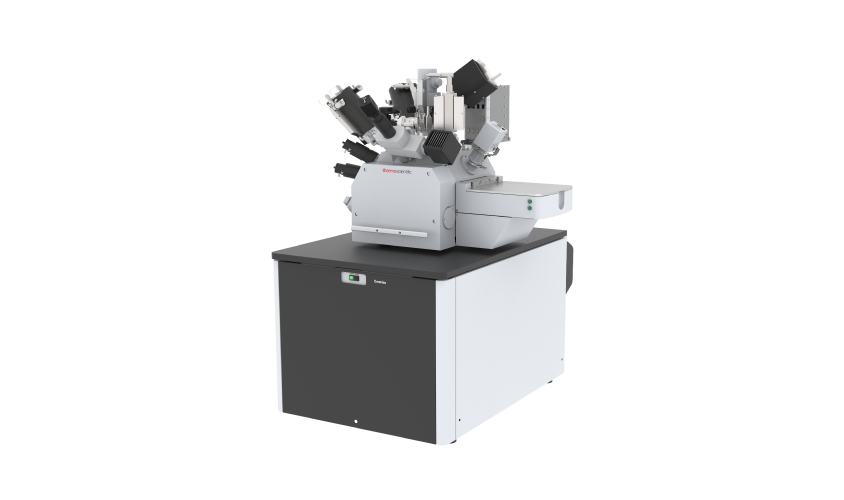
Micro-computed tomography (microCT)
Having the ability to efficiently produce quantitative 3D images of nearly any sample, micro-computed tomography (microCT) has become a standard tool for materials science research. As the reconstructions are generated with non-destructi...
Read more
Sample Vitrification in Electron Microscopy
Vitrification forms an amorphous solid that does little to no damage to the sample structure. This is a critical technique for cellular and structural biology research, where samples are cooled so rapidly that the surrounding water molec...
Read more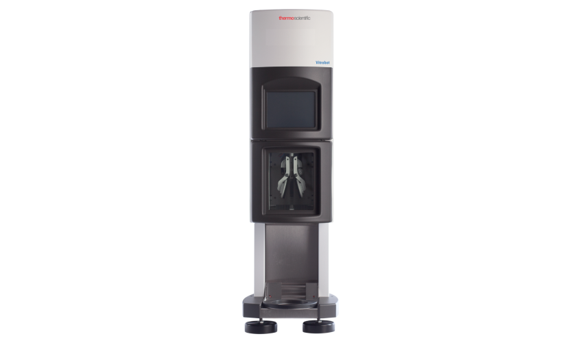
Detectors for Electron Microscopy
Thermo Scientific Pathfinder X-ray microanalysis for SEM/EDS and SEM/WDS prevents many of the difficulties found in traditional elemental-based X-ray microanalysis. Pathfinder software classifies the chemical phases in your sample straig...
Read more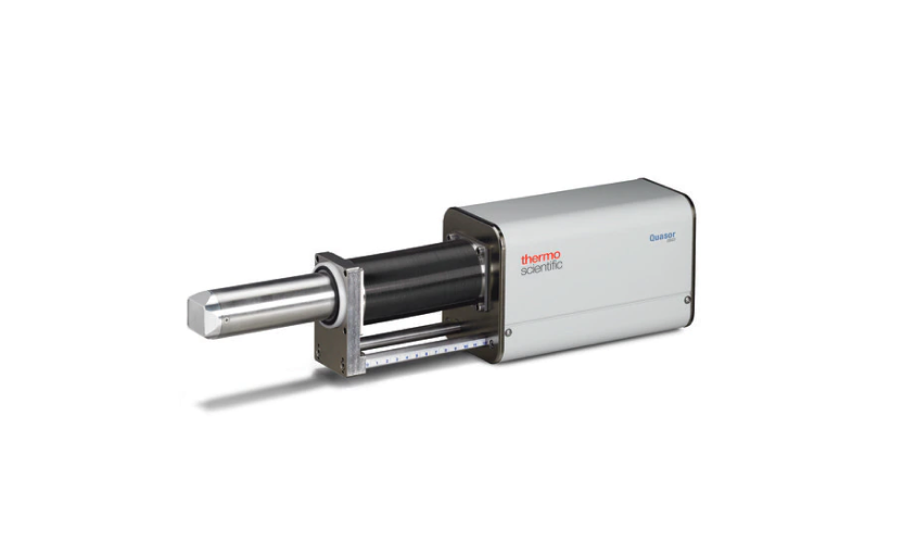
Electron Microscopy Applications
electron-microscopy
For both techniques, electrons are used to acquire images of samples. SEMs use a specific set of coils to scan the beam in a raster-like pattern and collect scattered electrons, providing information on surface and composition. TEM uses transmitted electrons passing through the sample, offering invaluable information on inner structure such as crystal structure and morphology. SEM resolution is limited to ~0.5 nm, while aberration-corrected TEMs achieve below 50 pm spatial resolution.
This depends on the type of analysis you want to perform. For surface information like roughness or contamination detection, choose SEM. For crystal structure, structural defects or impurities, TEM is the only way to do so.
Evaluating the quality of coatings requires detailed morphological analysis. SEMs use backscatter electron (BSE) imaging to capture high-magnification, high-contrast images that show exactly where a coating has or has not been applied. Uncoated areas as small as several micrometers can be the starting points for corrosion.
In the case of a SEM, three types of signal are typically detected: backscattered electrons (BSE), secondary electrons (SE), and characteristic X-rays (EDS). Each type carries different useful information about the sample.
BSE are reflected after elastic interactions and come from deeper regions of the sample – they show high sensitivity to differences in atomic number. SE originate from the atoms of the sample through inelastic interactions and come from surface regions, providing detailed surface topography information.
ChemiSEM Technology provides full control over all SEM and EDS functions within a single user interface. It is always on and continuously collects the EDS signal during SEM imaging. It enables faster data acquisition through machine learning-based segmentation, reliable results over a wide range of operating conditions, and simplified operation accessible to all scientists and engineers.
ChemiPhase is a ChemiSEM Technology feature that allows phase analysis on areas of interest using a big data approach to detect all statistically significant spectra within the datacube. It is a comprehensive, unbiased statistical engine that avoids erroneous results from overlapping peaks or insufficient intensities, making phase characterization straightforward and intuitive.
Single particle cryo-EM or single particle analysis is an increasingly popular cryo-EM technique that allows you to investigate biomolecules at near- and atomic resolutions, unraveling dynamic biological processes and the structure of biomolecular complexes/assemblies. In single particle cryo-EM, purified proteins or protein complexes are suspended in amorphous (vitreous) ice through rapid plunge freezing, which preserve the samples’ native structures. Transmission electron microscopy (TEM) is then used to collect numerous 2D snapshots of the samples. As the proteins are oriented randomly within the ice, these images show the sample at various angles and can be recombined into a high-resolution 3D reconstruction of the sample.
Cryo-electron tomography (cryo-ET) enables three-dimensional visualization of cells, organelles and macromolecular complexes in their near-native state. By combining cryogenic preservation with tilt-series acquisition and computational reconstruction, cryo-ET bridges cellular context with molecular resolution, revealing biological architecture as it exists in situ.
Continued innovation in life science microscopy, spanning advanced technologies, precision engineering and integrated workflows, is enabling this transformation and this is expanding the impact of cryo-ET across structural biology, cell biology and drug discovery research worldwide.
MicroED is a technique that allows for fast, high-resolution structural determination of small molecules and proteins. Atomic details can be extracted from individual nanocrystals (<200 nm in size), even in a heterogeneous mixture. MicroED data is acquired on a cryo-transmission electron microscope (cryo-TEM), using electrons as the incident beam.
Since MicroED is a diffraction technique, samples need to be crystalline, and the crystallization process is the same as for X-ray crystallography. However, much smaller crystals can be used in MicroED because the interaction of the crystal with electrons is much stronger than it is with X-rays. Crystals that are only 100 nm in size can readily be analyzed. This may significantly shorten the sample preparation process and allows for the analysis of crystals that are too small to diffract with other methods. Data collection is completed in only a few minutes, and 3D structures can be determined at atomic resolution.